How to Trace and Map Keypad Layouts on Mobile Phone PCBs
Tracing and mapping keypads on a mobile phone printed circuit board (PCB) is an essential skill for hardware troubleshooting. By understanding the connections of each key, technicians can diagnose malfunctioning buttons or keypads efficiently.
Using a Schematic Diagram
The fastest and most reliable method for tracing a keypad layout is using a schematic diagram. This diagram provides a visual guide of how each key is connected on the PCB. In a schematic, keypad switches are organized into rows and columns, making it easier to identify the paths and connections for each key.

Step-by-Step Method
Follow these steps to trace and map the keypad layout:
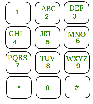
- Locate the keypad section: Find the keypad section on the schematic diagram of the mobile phone.
- Identify rows and columns: Observe how each key is grouped along rows and columns.
- Trace the connections: Using a multimeter set to the X1 resistance range, check each key by connecting probes across the corresponding row and column connections.
- Mark the PCB: Once the connection is confirmed on the schematic, trace and map the same lines directly on the mobile phone PCB.
- Practice and refine: With repeated practice using schematic diagrams, you will develop the ability to trace keypads even when no schematic is available.

Tips for Beginners
- Always start by identifying rows and columns clearly before testing with a multimeter.
- Use consistent probe placement to avoid misreading resistance values.
- Label each mapped key directly on the PCB or a reference sheet to avoid confusion.
- Practice on different phone models to improve your tracing skills.
Conclusion
Tracing and mapping keypads is a foundational skill for mobile hardware repair. By using schematic diagrams and a multimeter, you can quickly identify faulty keys, verify connections, and confidently troubleshoot keypads on any mobile phone PCB.